


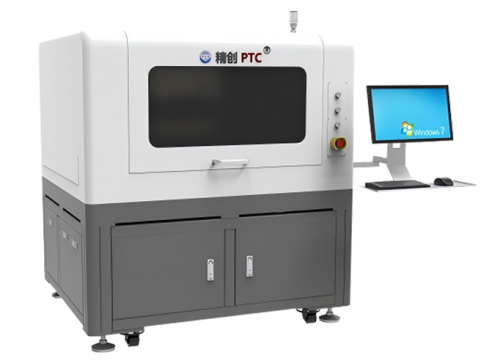
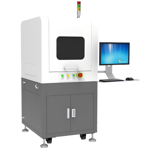
At the 2025 World Semiconductor Conference and Expo, a key technological device attracted much attention — the ultrasonic scanning microscope. This equipment is becoming a "capable assistant" in quality control and inspection links during semiconductor manufacturing.
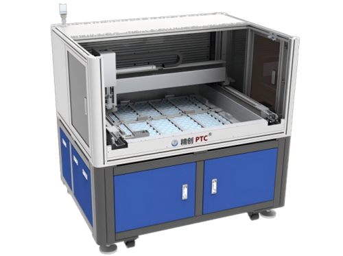
As the world's latest generation of ultrasonic testing equipment, the ultrasonic scanning microscope works based on the differences in ultrasonic acoustic impedance, sound wave absorption, and reflection degrees among different materials. By emitting short waves into the interior of a sample, at the interfaces of different materials, varying reflection energy or phase information is generated due to differences in impedance. This information is then used to construct images of the sample's internal structure, enabling the detection of structures and defects in semiconductors and components, as well as qualitative analysis of materials. It has significant advantages: it can perform layered and multi-layer scanning, conduct intuitive image analysis and defect measurement statistics, carry out non-destructive testing of chips without damaging their internal structures, and is sensitive to bonding layers, being able to penetrate most materials.
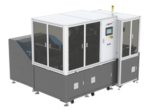
In the semiconductor industry, ultrasonic scanning microscopes are widely used. They are indispensable in links such as incoming quality control (IQC), failure analysis (FA), quality control (QC), quality assurance and reliability (QA/rel), and research and development (R&D). For example, in chip manufacturing, they can detect internal lattice structures, impurity particles, internal cracks, delamination defects, voids, and bubbles in materials. The ECHO LS™ ultrasonic microscope from SONIX, for instance, can detect defects as small as 0.05μm, performing excellently in semiconductor and integrated circuit manufacturing, packaging, and testing. It can effectively detect internal cracks, bubbles, and other defects in devices, improving production efficiency and output.
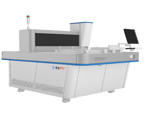
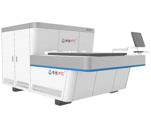
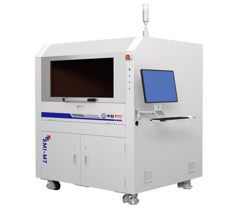
Currently, domestic ultrasonic scanning microscopes are also continuously developing. Products from Kunshan Zhongchuang Semiconductor Technology Co., Ltd. have obtained multiple patents, reaching the advanced level of the industry, and can develop customized models according to user needs. As the semiconductor industry's requirements for product quality continue to rise, ultrasonic scanning microscopes will continue to assist the industry's development, playing a more critical role in ensuring product quality and promoting technological innovation.


 Home
Home Products
 Telephone
 Message

