


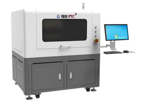
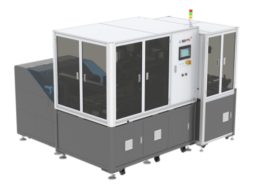
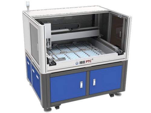
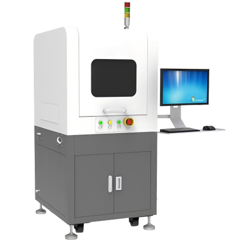
What is an Exposure Machine?
An exposure machine is a core device in precision manufacturing fields such as microelectronics, semiconductors, photovoltaics, and flat-panel displays. It primarily functions to transfer preset patterns (e.g., circuit patterns, precision structures) onto the surface of workpieces (such as wafers, PCB boards, photoresist coatings), enabling high-precision patterning. It is the key executor of the lithography process (a critical step in pattern transfer).
Equipment Types of Exposure Machines
Exposure machines are categorized based on application scenarios, light source types, and exposure methods, as follows:
1. Classification by Application Field
Semiconductor exposure machines: Used for transferring circuit patterns onto wafer surfaces in chip manufacturing, serving as the "core equipment" in integrated circuit (IC) production. They require extremely high resolution and alignment accuracy (nanoscale).
- Representative technologies: Extreme Ultraviolet (EUV) exposure machines, Deep Ultraviolet (DUV) exposure machines (e.g., ArF, KrF light sources).
Photovoltaic exposure machines: Applied in patterning processes of photovoltaic cells (e.g., PERC, TOPCon, HJT cells) such as electrode patterns and grid lines. They prioritize a balance between efficiency and cost, with lower resolution requirements than semiconductor equipment (micron-scale).
Flat-panel display exposure machines: Used in processing array substrates and color filter substrates of LCD, OLED, and other display panels. They need to adapt to large-size substrates (e.g., G8.5 generation substrates exceeding 2 meters) while balancing precision and productivity.
PCB exposure machines: Designed for transferring circuit patterns onto printed circuit boards (PCBs). Specialized models are available for different PCB types (e.g., rigid boards, flexible boards), with micron-scale resolution.
2. Classification by Exposure Method
Contact exposure machines: The photomask (a template carrying patterns) directly contacts the workpiece coated with photoresist. Pattern transfer is achieved through light irradiation.
- Features: Simple structure and low cost, but prone to photomask wear and low precision (suitable for low-end PCBs, semiconductor packaging, etc.).
Proximity exposure machines: The photomask maintains a small gap (typically 10-50μm) from the workpiece surface to avoid direct contact and reduce wear.
- Features: Higher precision than contact-type machines but limited resolution due to diffraction effects (suitable for mid-to-low-end semiconductors and PCBs).
Projection exposure machines: Patterns on the photomask are reduced and projected onto the workpiece surface via optical systems, making them the mainstream type in high-precision fields.
- Features: Non-contact operation and high resolution (up to nanoscale). They include step-and-repeat, scan, and step-and-scan types, among which step-and-scan is the core technology for high-end semiconductor exposure machines (e.g., ASML’s EUV exposure machines).
3. Classification by Light Source Type
- Ultraviolet (UV) exposure machines: Equipped with low-pressure mercury lamps (254nm) or high-pressure mercury lamps (365nm), suitable for PCBs and low-end semiconductors.
- Deep Ultraviolet (DUV) exposure machines: Using KrF (248nm) or ArF (193nm) light sources, they can achieve 10nm-level processes through immersion technology (filling pure water between the lens and wafer to improve resolution), serving as the mainstay in current semiconductor manufacturing.
- Extreme Ultraviolet (EUV) exposure machines: With a light source wavelength of 13.5nm, they can directly achieve processes at 7nm and below, acting as core equipment for high-end chips (e.g., 5nm, 3nm). They involve extremely high technical difficulty (only ASML globally can mass-produce them).
- Laser direct writing exposure machines: No photomask is required; patterns are directly "drawn" via laser beam scanning. They offer high flexibility and are suitable for small-batch, high-precision scenarios (e.g., semiconductor R&D, precision processing of photovoltaic cells).
Working Principle of Exposure Machines
The core principle of an exposure machine lies in using light-induced chemical reactions (photoresist photosensitivity) to achieve pattern transfer. The specific process is as follows:
1. Pretreatment: The workpiece surface (e.g., wafer, PCB) is uniformly coated with photoresist (a photosensitive material sensitive to specific wavelengths of light) and cured by baking.
2. Pattern alignment: The photomask (or "virtual pattern" in laser direct writing) is precisely aligned with the workpiece surface (alignment accuracy directly affects final pattern precision, reaching nanoscale in high-end equipment).
3. Exposure: The light source (e.g., UV, EUV) irradiates the photomask, where pattern areas transmit light and non-pattern areas block it (or in laser direct writing, the laser scans directly along the pattern path). This causes chemical changes in the photoresist (positive photoresist dissolves in developer after exposure, while negative photoresist does the opposite).
4. Development and post-processing: After exposure, unexposed (or exposed) photoresist is removed using a developer, exposing the workpiece surface to be processed. Subsequent processes such as etching or ion implantation permanently transfer the pattern to the workpiece.
In summary, exposure machines are the "eyes" of precision manufacturing. Their technical level directly determines the precision and performance of products such as chips, photovoltaic cells, and display panels. Different types of exposure machines are optimized for light sources, alignment methods, and precision based on application scenarios, while their core working logic"light-induced chemical changes for pattern transfer"—making them key equipment for "micro-world processing" in modern industry.


 Home
Home Products
 Telephone
 Message

